Leakage, Dynamic & Static Power

This post dives into the details of power loss and how to avoid it, by studying a CMOS based NOT gate.

Let us take a look at what power management means, and why the Clock frequency and Voltage has such an influence on the power consumption. To keep things simple, consider the following -
- Digital Circuits are composed of Logic Gates.
- Logic Gates are composed of Transistors.
- The Transistors used are composed of CMOS (
nMOSandpMOS) transistors.
The NOT Gate
To guide our discussion further, we will focus on the NOT Gate as implemented using the CMOS as in Figure #1
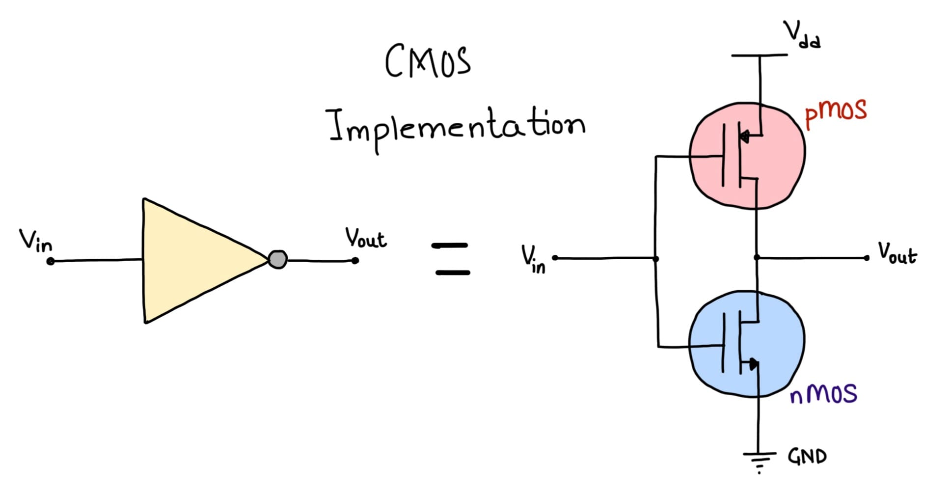
\( V_{out} \) is inversion of \( V_{in} \). When pMOS is ON, nMOS is OFF and vice-versa. This is the Key!
Power leaks in two forms, one is when there is a transition between the levels and the second is to keep the circuit active (in its current state). These are termed as Dynamic and Static power respectively.
Leakage Power
We'll continue our discussion using the NOT Gate's CMOS model. The idea is, when one MOSFET is OFF, the other is ON. So at any given point, the Vout is either pulled high to the Vdd (the supply voltage) or is pulled low to the GND (ground).
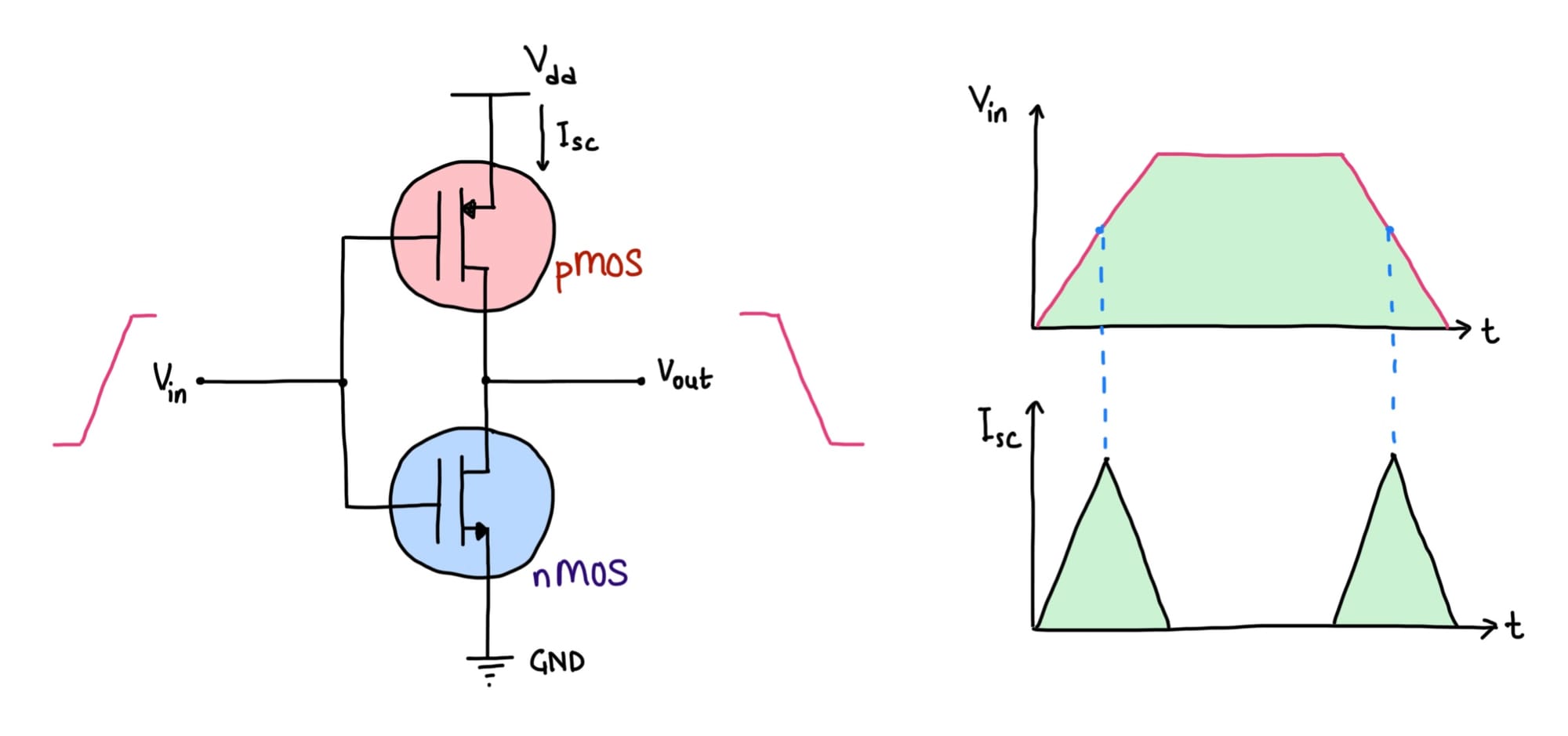
Vin transition.Think about what will happen when Vin is transitioning from 1 to 0 or from 0 to 1. Both MOSFETs will be partially ON (conducting) for a brief period of time during the transition and there would be some current going from the Vdd to the GND. This current is noted as Isc in Figure #2. Figure also shows the current conduction correlated with the voltage transition. Remember, Power (P) is a product of Voltage (V) and Current (I), so briefly there is power dissipated as a result of the transition. If the Vin was to have a frequency f at which it is changing, we would have the Power dissipation as follows \[ P_{leakage} = f.V_{dd}.I_{sc} \]
Role of Capacitive Loading
Let's now think a little bit beyond the NOT gate. The Output Vout must be driving some other CMOS... (because circuits are made of many gates and the output of one Gate drives another.) as in Figure #3.
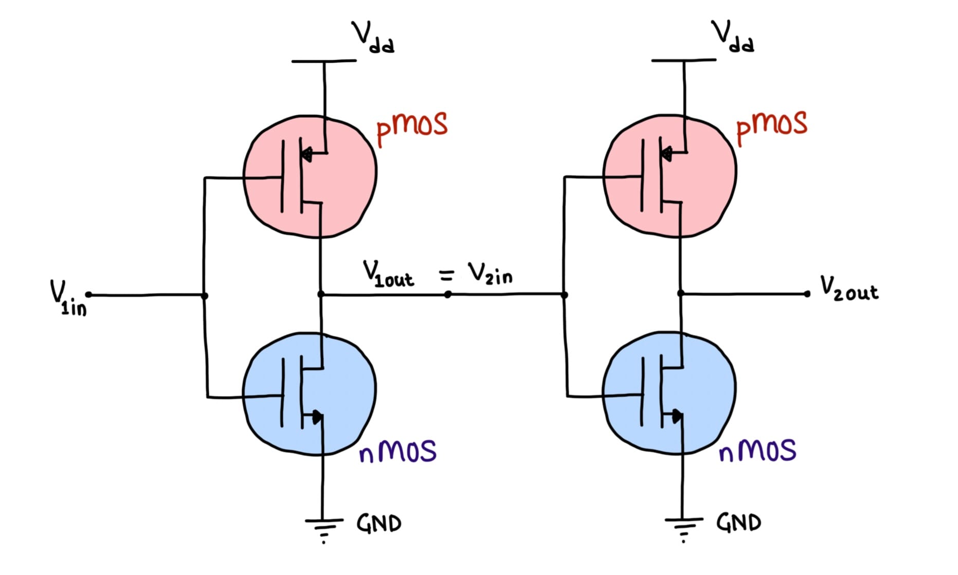
The GATE (the control terminal where V1in and V2in are connected) terminal on the MOSFET serves as a capacitor of sorts. During the level transition, this capacitor will change and discharge. The effective model then becomes as in Figure #4.
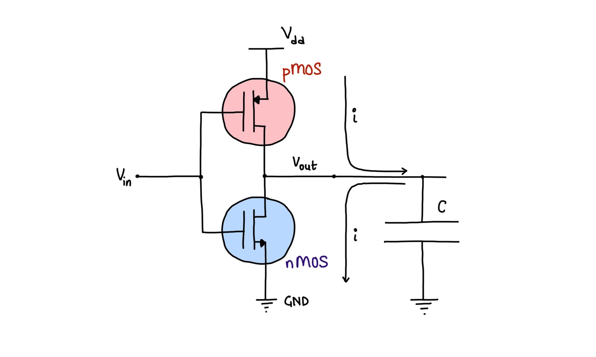
The current (represented by i) is transient and only exists during the level transition. This then by the basics of electrical circuit analysis comes down to the following:
\[ i = \frac{dv_c}{dt}.C \]
Which is to say, the current is the rate of change of the Voltage (vc) across this Capacitor times the Capacitance value. The Capacitance value is a function of the manufacturing process and is known. This becomes more interesting when we question the Energy and power this would result.
\[ E = \frac{V.C}{2} \]
If we adapt this equation to the Changing Voltage for the model in Figure #4 it becomes - \[ E = \int_{0}^{V_{dd}}V_{dd}.C.\frac{dv_c}{dt}.dt = C.V_{dd} ^ 2\]
Power is Energy per unit time. The Power consumption then becomes -
\[ P = \frac{E}{\Delta t} \] It is safe to assume that Vin will change as per some frequency f on average. The dynamic power then becomes \[ P_{cap} = f.E = f.C.V_{dd} ^ 2 \] Note that, \[ f = \frac{1}{\Delta t} \]
Further, not every CMOS transistor is transitioning every second. So, we throw in something call switching factor(\( \alpha \) ) which represents how many CMOS transistors changes state every second. Final power equation then becomes \[ P_{cap} = \alpha.f.C.V_{dd} ^ 2 \]
Insights from the Capacitive Power Equation
We can conclude the following from the power equation above
- Higher rate of transition (
f) will result in more power. - Higher
Vddwill result in more power. - Higher
Cwill result in more power.
As you can guess, lower frequency (f), lower supply voltage (Vdd) and lower capacitance C would mean lower power numbers. Now you can reason about why there is a push to operate at lower voltages and frequency. Capacitance is a function of technology on which the transistors are manufactured.
Dynamic Power
Dynamic power is power that is lost due to changing states. It is represented as a sum of the Leakage and Capacitive Power.
\[ P_{dyn} = P_{leakage} + P_{cap} \]
Saving Dynamic Power
The Power equation above is a very powerful one. Adjusting various variables in it leads to huge power saving.
Clock gating
One of the obvious ways in which dynamic power can be saved if the circuit is not actively used (but we anticipate it will be used soon... Like a CPU doesn't have a workload on it but might get one in immediate future) is to cut the clock to the circuit. This makes the frequency zero. Guess what the dynamic power becomes? ZERO!
DVFS
The second method is to actively monitor the workload on a circuit and set it's Voltage and Frequency accordingly. This is called DVFS - Dynamic Voltage and Frequency Scaling.
This technique is deployed in circuits with processors on it. Typically, there is a dedicated state-machine keeping track of the workload and setting the Voltage and Frequency accordingly. These Voltage-Frequency combinations are predefined by the circuit manufacturer and captured as a table. The process by which these are discovered is called - Characterisation.
Static Power
Even if there are no state transition occurring (Vin is not changing). The circuit will consume some power. This is dictated by the semiconductor physics and is dependent on the manufacturing process. Based on semiconductor physics this is defined as \[ P_{static} = V_{dd}.I_{static}.e^{-\frac{q.V_T}{K.T} - 1} \]
There is lot going on here, the \( V_T \) is the junction voltage, \( T \) is the temperature, \( K \) is the Boltzmann constant and \( q \) is the electronic charge. The only thing we can control to some degree from the equation is \( T \) and \( V_{dd} \).
To save static power, we can turn off a circuit if it is not in use and we anticipate that it won't be used in near future. This is called - Power Gating.
Total Power
The total power obviously, is sum of all the components leading to power loss - \[ P_{total} = P_{dyn} + P_{static}= P_{leakage} + P_{cap} + P_{static} \] and when expanded becomes \[ P_{total} = f.V_{dd}.I_{sc} + \alpha.f.C.V_{dd} ^ 2 + V_{dd}.I_{static}.e^{-\frac{q.V_T}{K.T} - 1} \]
This is the master equation you should brain tattoo in terms of reasoning about power!
Discussion